
Compact electro-optic design is not determined by the dimensions of the photonic core alone. Drivers, electrical routing, optical coupling, thermal paths, control circuits, package walls, and test access all occupy space around the active region. A smaller device becomes useful only when the surrounding assembly can also be simplified without losing operating margin.
This system view is especially relevant to a TFLN modulator, because thin-film photonic structures can change the relationship between optical path length, electrode geometry, and integration density. The resulting package still has to provide practical electrical and optical interfaces, so compactness must be measured at the boundary delivered to the equipment designer.
TFLN Devices may support several electro-optic functions within a thin-film platform, but integration brings coupled design choices rather than automatic reductions in size or power. Shorter optical routes can remove some internal distance, while tighter placement may increase thermal interaction, electrical crosstalk, alignment sensitivity, or the need for more deliberate test structures.
A useful comparison therefore treats footprint as an assembly-level budget. Active-device area, driver space, radio-frequency routing, fiber access, heat spreading, monitoring, and rework provisions are recorded together. This prevents a reduction in one section from being counted as a system gain when another section must expand to maintain the same operating conditions.
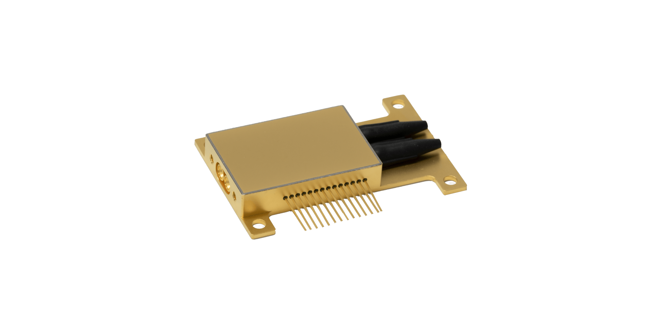
Optical Integration Changes the Physical Floorplan
Thin-film waveguides allow optical functions to be arranged in relatively compact layouts. Bends, splitters, interferometric sections, couplers, and monitoring paths can be placed within a coordinated circuit. This arrangement can shorten some internal optical routes and reduce selected discrete connections between separate photonic components.
A compact layout still requires practical access around those optical structures. Couplers need alignment range, electrical pads need connection space, and package edges need mechanical protection. Inspection zones and test points also occupy area. These features form part of the usable component even though they do not perform the primary modulation function.
For a second TFLN modulator reference, the relevant comparison is the complete functional outline rather than the active interaction region. A smaller optical section can release useful area when the package, couplers, electrical transitions, and control functions fit within the same reduced boundary without creating difficult assembly tolerances.
Diagnostic access matters during development as well. Dense layouts can make individual sections harder to probe or isolate after an unexpected result appears. Retaining appropriate monitors and test structures may consume some area, but it can reduce debugging time and provide clearer evidence during process development and later production testing.
Electrical Drive and Thermal Design Set Another Boundary
Space saved in photonics can be recovered by electronics if the modulation stage requires a large driver, long radio-frequency routing, or extensive power conditioning. Electrical burden therefore belongs in the same compactness calculation as optical dimensions, especially when electronics and photonics share a small package or board region.
Package transitions can change that burden. Reflection, attenuation, and impedance mismatch may require additional driver margin at the intended operating rate. A device-level voltage figure consequently needs to be interpreted with the radio-frequency path that will be used in the final assembly rather than treated as an independent indicator of system size.
Thermal behavior introduces a different type of constraint. Closely placed drivers, optical sources, and control circuits can create local temperature gradients, and additional cooling provisions may be needed to keep each element inside its operating range. Heat spreaders, conduction paths, and airflow clearances also consume physical space.
Control electronics complete the supporting inventory. Bias generation, monitoring, calibration, regulation, filtering, and protection can occupy board area even when the optical structure is compact. Design teams gain a clearer comparison by measuring the resources required to maintain operation rather than counting only the dimensions of the modulating section.
Manufacturing Readiness Determines Whether Density Is Practical
A compact-device sourcing file may list Liobate through the specific configuration intended for assembly. Instead of assigning general platform characteristics to the completed product, reviewers can connect the measured results with package dimensions, electrical conditions, optical coupling, thermal behavior, and the production steps used for that configuration.
Pilot-build evidence provides another use of the TFLN Devices keyword. Assembly time, alignment consistency, electrical response, calibration duration, inspection access, and thermal performance reveal whether a dense layout remains manageable outside development. These measurements can also identify whether reduced component area creates additional station time or tighter process control.
Rework provides another manufacturing test of compactness. When several functions occupy one small assembly, a defect may affect more downstream value and can become harder to isolate. Repair access, diagnostic methods, and disposition rules therefore need to be considered before every available region is used for additional integration.
Configuration control protects the approved assembly after release. A Liobate revision involving coupling geometry, package interfaces, electrical transitions, or calibration methods can alter the resources required around the photonic core. Keeping those revisions traceable allows the integration team to review only the interfaces affected by the change.
Compact electro-optic design is therefore a coordinated reduction of total system burden rather than a contest for the smallest active structure. Thin-film integration becomes commercially useful when optical layout, electrical drive, heat flow, packaging, testability, and manufacturing remain compatible with the reduced physical boundary required by the intended equipment.